In the previous pair of installments in this series, you built a simple Verilog demonstration consisting of an adder and a few flip flop-based circuits. The simulations work, so now it is time to put the design into a real FPGA and see if it works in the real world. The FPGA board we’ll use is the Lattice iCEstick, an inexpensive ($22) board that fits into a USB socket.
Like most vendors, Lattice lets you download free tools that will work with the iCEstick. I had planned to use them. I didn’t. If you don’t want to hear me rant about the tools, feel free to skip down to the next heading.
Hiccups with Lattice’s Toolchain
 Still
here? I’m not one of these guys that hates to sign up for accounts. So
signing up for a Lattice account didn’t bother me the way it does some
people. What did bother me is that I never got the e-mail confirmation
and was unable to get to a screen to ask it to resend it. Strike one.
Still
here? I’m not one of these guys that hates to sign up for accounts. So
signing up for a Lattice account didn’t bother me the way it does some
people. What did bother me is that I never got the e-mail confirmation
and was unable to get to a screen to ask it to resend it. Strike one.I had tried on the weekend and a few days later I got a note from Lattice saying they knew I’d tried to sign up and they had a problem so I’d have to sign up again. I did, and it worked like I expected. Not convenient, but I know everyone has problems from time to time. If only that were the end of the story.
I was impressed that Lattice does support Linux. I downloaded what appeared to be a tgz file. I say appeared because tar would not touch it. I examined the file and it looked like it was gzipped, so I managed to unzip it to a bare file with a tar extension. There was one problem: the file wasn’t a tar file, it was an executable. Strike two. I made it executable (yes, I’m daring) and I ran it. Sure enough, the Lattice installer came up.
Of course, the installer wants a license key, and that’s another trip to the Web site to share your network card’s MAC address with them. At least it did send me the key back fairly quickly. The install went without incident. Good sign, right?
I went to fire up the new software. It can’t find my network card. A little Internet searching revealed the software will only look for the eth0 card. I don’t have an eth0 card, but I do have an eth3 card. Not good enough. I really hated to redo my udev rules to force an eth0 into the system, so instead I created a fake network card, gave it a MAC and had to go get another license. Strike 3.
I decided to keep soldiering (as opposed to soldering) on. The tool itself wasn’t too bad, although it is really just a simple workflow wrapper around some other tools. I loaded their example Verilog and tried to download it. Oh. The software doesn’t download to the FPGA. That’s another piece of software you have to get from their web site. Does it support Linux? Yes, but it is packaged in an RPM file. Strike 4. Granted, I can manually unpack an RPM or use alien to get a deb file that might work. Of course, that’s assuming it was really an RPM file. Instead, I decided to stop and do what I should have done to start with: use the iCEStorm open source tools.
TL;DR: It was so hard to download, install, and license the tool under Linux that I gave up.
Programming an FPGA Step-by-Step
Whatever tools you use, the workflow for any FPGA is basically the same, although details of the specific tools may vary. Sometimes the names vary a bit, too. Although you write code in Verilog, the FPGA has different blocks (not all vendors call them blocks) that have certain functions and methods they can connect. Not all blocks have to be the same either. For example, some FPGAs have blocks that are essentially look up tables. Suppose you have a look up table with one bit of output and 16 rows. That table could generate any combinatorial logic with 4 inputs and one output. Other blocks on the same FPGA might be set up to be used as memory, DSP calculations, or even clock generation.Some FPGAs use cells based on multiplexers instead of look up tables, and most combine some combinatorial logic with a configurable flip flop of some kind. The good news is that unless you are trying to squeeze every bit of performance out of an FPGA, you probably don’t care about any of this. You write Verilog and the tools create a bitstream that you download into the FPGA or a configuration device (more on that in a minute).
The general steps to any FPGA development (assuming you’ve already written the Verilog) are:
- Synthesize – convert Verilog into a simplified logic circuit
- Map – Identify parts of the synthesized design and map them to the blocks inside the FPGA
- Place – Allocate specific blocks inside the FPGA for the design
- Route – Make the connections between blocks required to form the circuits
- Configure – Send the bitstream to either the FPGA or a configuration device
Constraints For Hardware Connected to Specific Pins (or: How does it know where the LED is?)
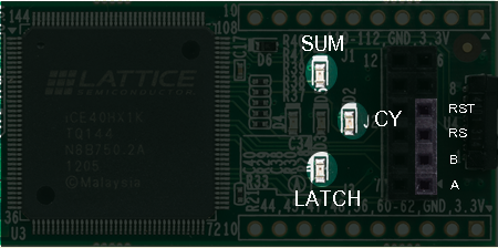
There is one other important point about placing. Did you wonder how the Verilog ports like LED1 would get mapped to the right pins on the FPGA? The place and route step can do that, but it requires you to constrain it. Depending on your tools, there may be many kinds of constraints possible, but the one we are interested in is a way to force the place and route step to put an I/O pin in a certain place. Without that constraint it will randomly assign the I/O, and that won’t work for a ready made PCB like the iCEStick.For the tools we’ll use, you put your constraints in a PCF file. I made a PCF file that defines all the useful pins on the iCEstick (not many, as many of you noted in earlier comments) and it is available on Github. Until recently, the tools would throw an error if you had something in the PCF file that did not appear in your Verilog. I asked for a change, and got it, but I haven’t updated the PCF file yet. So for now, everything is commented out except the lines you use.
Here’s a few lines from the constraint file:
set_io LED3 97  # red
set_io LED4 96  # red
set_io LED5 95  # green
 Every
external pin (including the clock) you plan to use must be defined in
the constraint file. Errors in the file can be bad too. Routing an
output to a pin that is connected, for example, directly to ground could
damage the FPGA, so be careful! The picture to the right shows the
configuration with my PCF file (the center LED and the one closest to
the FPGA chip just blink and are not marked in the picture). Keep in
mind, though, you could reroute signals any way that suited you. That
is, just because LED1 in the Verilog is mapped to D1 on the board,
doesn’t mean you couldn’t change your mind and route it to one of the
pins on the PMOD connector instead. The name wouldn’t change, just the
pin number in the PCF file.
Every
external pin (including the clock) you plan to use must be defined in
the constraint file. Errors in the file can be bad too. Routing an
output to a pin that is connected, for example, directly to ground could
damage the FPGA, so be careful! The picture to the right shows the
configuration with my PCF file (the center LED and the one closest to
the FPGA chip just blink and are not marked in the picture). Keep in
mind, though, you could reroute signals any way that suited you. That
is, just because LED1 in the Verilog is mapped to D1 on the board,
doesn’t mean you couldn’t change your mind and route it to one of the
pins on the PMOD connector instead. The name wouldn’t change, just the
pin number in the PCF file.Configuring an FPGA
Different FPGAs use different technology bases and that may affect how you program them. But it all starts with a bitstream (just a fancy name for a binary configuration file). For example, some devices have what amounts to nonvolatile memory and you program the chip like you might program an Arduino. Usually, the devices are reprogrammable, but sometimes they aren’t. Besides being simpler, devices with their own memory usually start up faster.However, many FPGAs use a RAM-like memory structure. That means on each power cycle, something has to load the bitstream into the FPGA. This takes a little time. During development it is common to just load the FPGA directly using, for example, JTAG. However, for deployment a microprocessor or a serial EEPROM may feed the device (the FPGA usually has a special provision for reading the EEPROM).
The FPGA on the iCEstick is a bit odd. It is RAM-based. That means its look up tables and interconnections are lost when you power down. The chip can read an SPI configuration EEPROM or it can be an SPI slave. However, the chip also has a Non Volatile Configuration Memory (NVCM) inside. This serves the same purpose as an external EEPROM but it is only programmable once. Unless you want to dedicate your iCEstick to a single well-tested program, you don’t want to use the NVCM.
The USB interface on the board allows you to program the configuration memory on the iCEstick, so, again, you don’t really care about these details unless you plan to try to build the device into something. But it is still good to understand the workflow: Verilog ➔ bitstream ➔ configuration EEPROM ➔ FPGA.
IceStorm
Since I was frustrated with the official tools, I downloaded the IceStorm tools and the related software. In particular, the tools you need are:- Yosys – Synthesizes Verilog
- Arachne-pnr – Place and Route
- Icestorm – Several tools to actually work with bitstreams, including downloading to the board; also provides the database Arachne-pnr needs to understand the chip
There are four command lines you’ll need to program your design into the iCEstick. I’m assuming you have the file demo.v and you’ve changed the simulation-only numbers back to the proper numbers (we talked about this last time). The arachne-pnr tool generates an ASCII bitstream so there’s an extra step to convert it to a binary bitstream. Here are the four steps:
- Synthesis:
yosys -p "synth_ice40 -blif demo.blif" demo.v - Place and route:
arachne-pnr -d 1k -p icestick.pcf demo.blif -o demo.txt - Convert to binary:
icepack demo.txt demo.bin - Configure on-board EEPROM:
iceprog demo.bin
./build.sh demoThis will do all the same steps using demo.v, demo.txt, and so on.
Try It Out
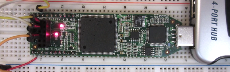
Once the board programs, it will immediately start operating. Remember, this isn’t a program. Once the circuitry is configured it will start doing what you meant it to do (if you are lucky, of course). In the picture below (and the video), you can see my board going through the paces. I have some buttons for the two adder inputs on one side and a reset button on the other. I also soldered some headers to the edge of the board.If you are lazy, you can just use a switch or a jumper wire to connect the input pins to 3.3V or ground. It looks like the device pins will normally be low if you don’t connect anything to them (but I wouldn’t count on that in a real project). However, I did notice that without a resistor to pull them down (or a switch that positively connected to ground) there was a bit of delay as the pin’s voltage drooped. So in the picture, you’ll see I put the switches to +3.3V and some pull down resistors to ground. The value shouldn’t be critical and I just grabbed some 680 ohm resistors from a nearby breadboard, but that’s way overkill. A 10K would have been smarter and even higher would probably work.

If it works, congratulations! You’ve configured an FPGA using Verilog. There’s still a lot of details to learn, and certainly this is one of the simplest designs ever. However, sometimes just taking that first step into a new technology is the hardest and you’ve already got that behind you.
Although you can do just about anything with an FPGA, it isn’t always the best choice for a given project. Development tends to be harder than microcontroller development (duplicating this project on an Arduino would be trivial, for example). Also, most FPGAs are pretty power hungry (although the one we used is quite low power compared to some). Where FPGAs excel is when you need lots of parallel logic executing at once instead of the serial processing inherent in a CPU.
FPGAs get used a lot in digital signal processing and other number crunching (like Bitcoin mining) because being able to do many tasks all at once is attractive in those applications. Of course, it is possible to build an entire CPU out of an FPGA, and I personally enjoy exploring unusual CPU architectures with FPGAs.
Then again, just because you can make a radio with an IC doesn’t mean there isn’t some entertainment and educational value to building a radio with transistors, tubes, or even a galena crystal. So if you want to make your next robot use an FPGA instead of a CPU, don’t let me talk you out of it.

0 comentarios:
Publicar un comentario